Additive manufacturing, or 3D printing as it is more commonly known, has revolutionized the modern production and design process. Initially developed in 1988 for rapid prototyping, additive manufacturing allows users to produce 3-dimensional physical objects directly from a computer file via layer-by-layer deposition. 3D printing is in stark contrast to traditional subtractive machining, such as CNC ‘computer numerical control’ machining, which relies on the removal of material from the substrate to produce the final product.
Additive manufacturing has many advantages over subtractive manufacturing, including reduced waste, increasing internal complexity, and eliminating the need for product-specific tooling. Unfortunately, the process melt involved in direct material deposition can also introduce defects, which have historically limited the usefulness of 3D printers to prototyping applications. These defects commonly result from a wide variety of sources, including melt pool instability, unexpected thermal deformation, environmental anomalies, and energy source fluctuations [1].
As a result, real-time monitoring techniques are essential to reduce scrap rates and therefore take full advantage of the potential benefits of additive manufacturing. Monitoring is especially important for metal 3D printing, not only because of the increased materials cost, but also because of the extremely high melt points. Luckily, the high temperatures utilized in metal 3D printing facilitate the integration of passive optical emission spectroscopy (OES). To better understand how OES can be integrated into a metal 3D printer, it is essential to gain a better understanding of the technology. For the sake of brevity, this application note will not go into detail about the fundamentals of OES itself, but if you would like more information on the subject, the Avantes application note titled ‘Plasma Diagnostics and Optical Emission Spectroscopy’ is recommended as reference on the topic.
Fundamentals of Metal 3D Printing
There are two primary methodologies employed for modern direct-metal-disposition 3D printers: laser powder bed fusion (LPBF) and directed-energy deposition (DED) [2] shown in Figure 1a and 1b respectively. Both of these techniques rely on a high-power laser, such as a CO2 or fibre laser, to fuse powdered metal in a pre-programmed pattern, layer by layer to construct the desired final product.
In LPBF, the whole platform is uniformly covered with a thin layer of powder, and the laser-scanned across the bed using galvanometric mirrors and an f-theta focusing lens. After each layer is fused, the platform is then shifted down, and the process is repeated until the construction of the final part is completed.
In DED, by contrast, the laser is focused on a permanent location with powder jets arranged at the appropriate angle to intersect at the focus of the laser. The material substrate is placed on an X-Y-Z translation stage and then scanned underneath the laser, layer-by-layer, during fabrication. At present, DED processing appears to be the dominant approach for direct metal deposition because of its high throughput, low waste, and larger build volume. However, LPBF is still used for high-precision applications when layering heights of less than 250mm are required.
As of today, the predominant choices for metal additive-manufacturing materials are Ti-6Al-4V, AlSi10Mg, steels (including stainless), and Inconels (Ni-alloys), for both LPBF and DED printers. However, while both deposition methods are capable of processing all of these materials, unlike LPBF, DED can also utilize wire feed technology. By using a wire feed, DED printer heads can use an even more comprehensive range of printer materials at a lower price.
For example, additive-manufacturing grade-316 stainless-steel powder costs, on average, twice as much per pound as grade-316 stainless-steel wire. The only downside to a wire is that the resolution of the system is then necessarily limited by the thickness of the wire, typically on the order of 1mm in diameter.


OES in Additive Manufacturing
Based on the geometry of the two primary additive-manufacturing processes for metal 3D printing shown above, it is easy to see why OES is such an attractive tool for process monitoring. Figure 2 shows an example in which an AvaSpec-ULS3648 was integrated into a DED printing head [3]. In this example, the light was collected by a fibre-optic cable oriented at a 60-degree angle relative to the laser’s optical axis.
In this particular application, the team at the University in Brussels was using OES to monitor the colour temperature of the melt pool. While the primary goal of this study was to develop a non-contact control system to prevent excessive heat transfer in the substrate to reduce the material tress, they also demonstrated that defects could be correlated to the presence of oxidation.
Similarly, it has also been demonstrated that monitoring the ratio of atomic emission lines can be directly correlated to the probability of structural defects, resulting from changes in atomic concentrations. For example, a team at Pennsylvania State University showed a direct correlation between atomic titanium and vanadium emissions and defect formation in Ti-6Al-4V [1]. Furthermore, a group out of the University of Michigan used OES to monitor chromium composition in H13 tool steel as a means of real-time material characterization, defect detection, process optimization, and process control [4]. As a result, more and more manufacturers are insisting on real-time monitoring to detected defects early in the production process.

Spectrometer Requirements
When collecting OES data for additive-manufacturing process monitoring, a spectrometer typically requires excellent spectral resolution to differentiate between similar atomic species. This makes the AvaSpec-ULS4096CL-EVO from Avantes an ideal choice for this application. This spectrometer is capable of providing 0.05 nm resolution within the range from 200 nm to 400 nm using a 3600-groove density grating.
Additionally, the AvaSpec-ULS4096CL-EVO has a CMOS detector array, which is ideal for high-light-level applications such as this one because of its superior linearity and dynamic range when compared to CCD detectors. When combined with Avantes’ proprietary high-speed electronic triggering, data transfer rates, and analogue and digital I/O capabilities, the AvaSpec series can provide seamless integration into high-speed inspection systems.
All of the AvaSpec spectrometers are also available as OEM modules so that they can be integrated into turnkey process control systems. These units can communicate via USB, Ethernet, and the native digital & analogue input/output capabilities of the Avantes AS-7010 electronics board, which provides for a superior interface with other devices.
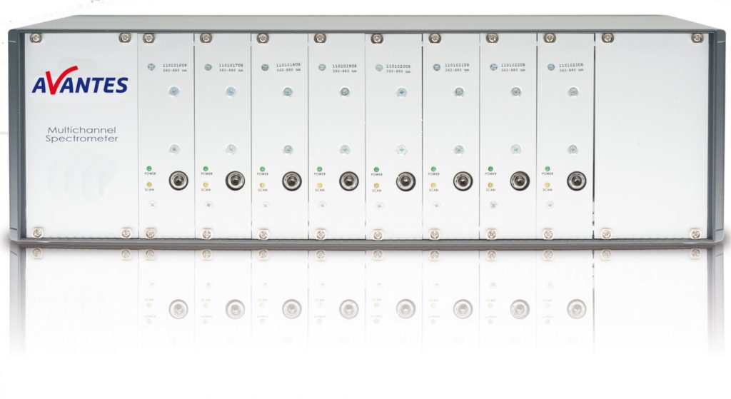
Additionally, the Avantes AvaSpec DLL software development application, with sample programs in Delphi, Visual Basic, C#, C++, LabView, MatLab, and other programming environments, enables users to develop code for their own applications. Furthermore, all Avantes spectrometers are designed to be multiplexed, or concatenated, enabling multichannel operation. This allows each spectrometer in the system to be optimized for spectral resolution over a small range, typically 200 nm – 300 nm, where the OES signal can be split evenly amongst them through the use of a multichannel fibre-optic bundle. This can provide for multiple redundant channels or ultra-high-resolution configurations covering a broader range. Avantes offers multi-channel configurations as individual modules or integrated into rackmount systems.
When integrating a spectrometer into a 3D printer head, it is also essential to choose a fibre-optic cable that is well suited for the particular environmental conditions. For harsh manufacturing environments, metal-jacketed fibre optic cables provide the highest level of protection from damage, but at the cost of flexibility. Therefore, it is also vital to take into consideration the mechanical constraints of the system, including cable routing and management, when selecting a fibre-optic cable.
In some cases, high-temperature (up to 500 degrees C) fibre assemblies may be necessary if the fibre tip is in close proximity to the melt pool. Avantes offers a variety of fibre cable configuration options to ensure that you can always find the ideal solution for your particular integration needs.
For more information about the full range of laboratory and OEM spectrometer options available from Avantes, contact us by completing this form, email us or call us at +31 (0)313 670 170. Our knowledgeable sales engineers are here to assist you.
Related Products
Related Pages
Resources
[1] Nassar, A.R., Spurgeon, T.J. and Reutzel, E.W., 2014, August. Sensing defects during directed-energy additive manufacturing of metal parts using optical emissions spectroscopy. In Solid Freeform Fabrication Symposium Proceedings (pp. 278-287). Austin, TX: University of Texas.
[2] Montazeri, M., 2019. Smart Additive Manufacturing: In-Process Sensing and Data Analytics for Online Defect Detection in Metal Additive- Manufacturing Processes.
[3] De Baere, D., Devesse, W., De Pauw, B., Smeesters, L., Thienpont, H. and Guillaume, P., 2016. Spectroscopic monitoring and melt pool temperature estimation during the laser metal deposition process. Journal of Laser Applications, 28(2), p.022303.
[4] Song, L. and Mazumder, J., 2011. Real-time Cr measurement using optical emission spectroscopy during direct metal deposition process. IEEE Sensors Journal, 12(5), pp.958-964.