Thin film is utilized across a wide range of industries including semiconductors, microelectronics, display technologies, and of course optical elements; this technology has enabled many of the technological breakthroughs taken for granted in modern times. While the end application of thin films can vary widely, what remains consistent is the need for precise control over the thickness of each layer during the epitaxial growth process.
With thin films, this can be especially challenging due to exactly how thin the layers are, typically ranging between 1 nm to 100 microns. One of the methods to precisely determine this thickness is by using a spectrometer. Presently there are three commonly used techniques to quantitate surface thicknesses on this scale: stylist profilometry, ellipsometry, and spectral reflectance (spectroscopy). While stylist profilometry technologies, including atomic force microscopy, are capable of sub-nanometer resolution, the contact nature of the techniques requires extremely long measurement times and can cause surface damage.
Ellipsometry and spectral reflectance, on the other hand, are both non-contact optical techniques which can scan large areas with little to no sample preparation. Ellipsometry is quite useful, but is typically larger and more expensive than spectral reflection because it requires off-axis measurement angles and multiple polarizations. Spectral reflectance, on the other hand, is a polarization-independent technique which is done at normal incidence, thereby greatly simplifying the cost and complexity of the system.
Effects of Film Thickness on Spectral Reflection
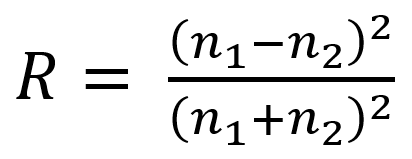
Whenever light propagates from one material to another, a certain percentage of that light is reflected back from the interface. While the equations that govern this interaction can be rather cumbersome, at normal incidence they reduce to a simplified expression which is solely dependent on the difference between the two indices of refraction. Equation 1 shows how, for non-absorbing materials, the reflectance (R) is equal to the square of the difference in the index (n1 and n2) divided by the square of the sum of the two indices. This simple equation is responsible for many of the physical phenomena you see in everyday life, including when you can see yourself in a transparent window when it’s dark. Additionally, many modern-day optoelectronics, including LEDs and laser diodes, utilize this relationship to improve performance and reduce cost.
When dealing with spectral reflectance from a single-layer thin film, there are now two different interfaces which will result in reflections: 1) the air-film interface and 2) the film-substrate interface. Depending on the thickness and the index of refraction of the thin film, this will cause the light reflected from each surface at a particular wavelength to have a slight phase difference, resulting in constructive or destructive interference. And, since the index of refraction of a material is wavelength dependent, this phase difference will vary across the spectrum of a broadband light source.
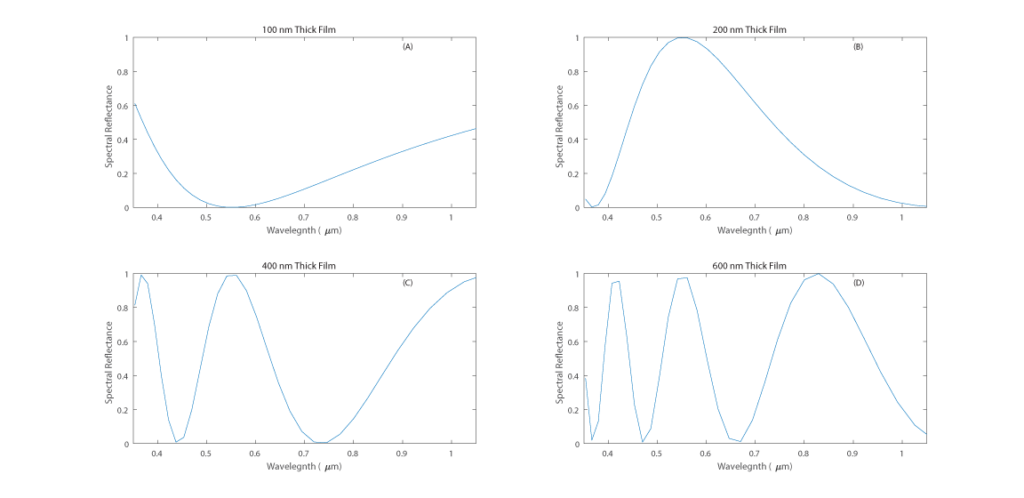
This wavelength-dependent interference pattern results in a chirped sinusoidal spectrum where the thicker the film, the higher the chirp frequency, as shown in Equation 2. In this equation, d represents the thickness of the film, n(l) the index of refraction as a function of wavelength, l the wavelengths, and I(l) the intensity as a function of wavelength.

While Equation 2 makes many simplifications and assumptions, it is beneficial for visualizing how the spectra will vary as a function of film thickness. Figure 1 shows an idealized example of such spectra for MgF2, which clearly indicates a chirped spectrum whose frequency increases with film thickness. In practice, most dielectric materials tend to absorb at least some of the light as it propagates through the material, and mathematically we can describe this property through the material’s complex index of refraction, where n represents the index of refraction, and k represents the absorption coefficient. It is important to note that, while mathematically the absorption coefficient is ‘imaginary’, it is a very real property which must be taken into account to accurately model the ‘real’ reflectance spectrum for a given film thickness.
Typical Thin Film Spectral Reflection Setup
The setup of a thin film spectral reflection measurement system is very similar to that of traditional reflectance except for the probe angle. As discussed earlier, in a thin film thickness experiment, the illumination and collection sources must be normal to the surface of the sample, in contrast to the 45-degree angle utilized in most reflectance measurements. This set-up includes a fibre-coupled spectrometer such as the AvaSpec-Mini2048CL or AvaSpec-ULS2048CL-EVO from Avantes, a fibre-coupled constant current tungsten light source such as the Avalight-HAL-S-Mini from Avantes and fibre-optic reflection probe such as the FCR-7UV200-2-ME from Avantes. For ultraviolet applications, a deuterium halogen light source such as the Avalight-DH-S can also be utilized. It is critical to ensure stable fixation of the probe tip and that the stand-off distance between the probe and reference is equal to the distance between the probe and samples. Figure 2 shows an example of a typical set-up.

Performing a Thin Film Measurement
The measurement process begins with the user first collecting a reference spectrum from an uncoated reference substrate to normalize the spectrometer and calculate an accurate reflection spectrum. Afterward, the reference substrate is replaced by the coated substrate, which is then measured under the same conditions. Once the reflectance spectrum has been measured, the AvaSoft software (Figure 3) can determine the film thickness.
To enable the most accurate measurement, it is essential that the substrate thickness and material, as well as the thin film design thickness and material, are input into the software. This data allows the software to access its database of material indices of refraction and absorption coefficients to correlate the measured reflectance spectrum with a theoretical curve of a given thickness. Figure 3 shows an example of a reflectance spectra for a 655 nm SiO2 thin film coated on a Si substrate, using the thin film measurement module within the AvaSoft software platform. In addition to the built-in library of common substrate and film materials, the user can also create their own “*.nk” file by entering in an array of indices (n) of refraction and coefficients of absorption (k) for each wavelength of interest.

Final Thoughts
By utilizing spectral reflectance for the thin film measurement process, engineers are now able to rapidly and cost-effectively test film thickness at all stages of the manufacturing process. Avantes offers a wide range of fibre-coupled miniature spectrometers, light sources, and probes, which when combined with their AvaSoft Thin Film software module, support measurements of single-layer thin films ranging from 10 nm to 50 μm in thickness with a 1 nm resolution. We offer optional thin film standards which provide sample uncoated and coated substrates for validation purposes and to verify the reliability and repeatability of the process as well.
The AvaSpec instruments are ideally suited to high-speed triggered, or continuous measurements such as those required in this application. Additionally, each spectrometer discussed above is also available as an OEM module and can be integrated into multichannel rack mount systems, which are perfectly adapted to thin film process monitoring systems. These instruments can communicate via USB, Ethernet, and the native digital & analogue input/output capabilities the Avantes AS-7010 electronics board provides for a superior interface with other devices. Additionally, the Avantes AvaSpec DLL software development application, with sample programs in Delphi, Visual Basic, C#, C++, LabView, MatLab, and other programming environments, enable users to develop code for thin-film applications. This software development kit is particularly useful for integration into an automated sampling system, or for analysis of complex multi-layer thin films requiring a customized code.
For more information about the full range of laboratory and OEM spectrometer options available from Avantes, feel free to contact one of our knowledgeable applications specialists, who are standing by to offer you the right setup for your application.
Why choose Avantes for your application?
- Market leader in developing high-end fibre-optic spectroscopy systems
- Nearly 30 years of experience and extensive industry and application knowledge
- The best engineers who perform feasibility studies to find the right solution for your application
- A support team that never sleeps and provides second-to-none customer service